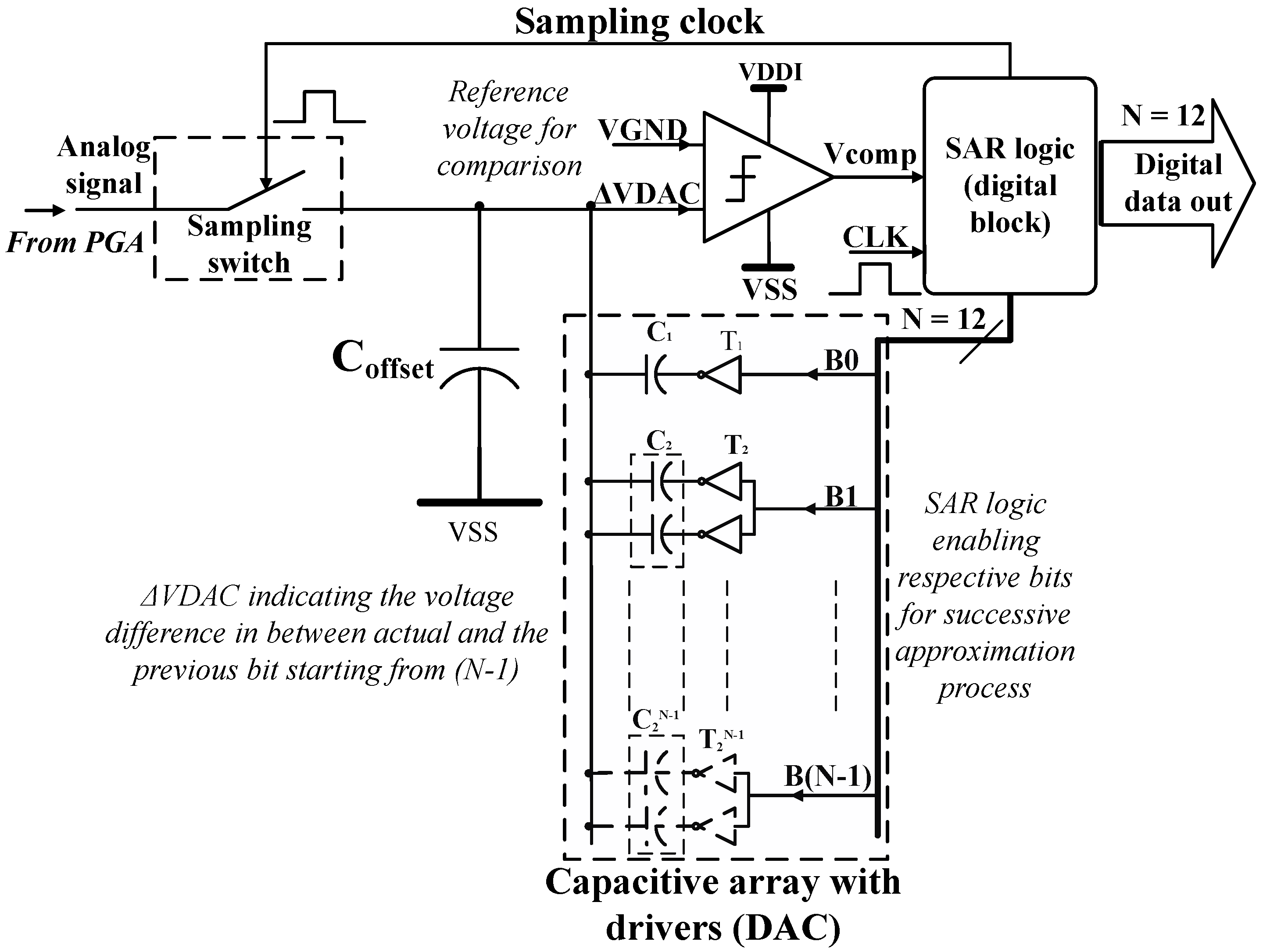
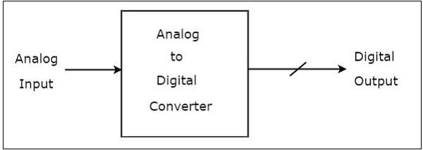
Sar Adc Block Diagram
Block Diagram of the SAR ADC IP.

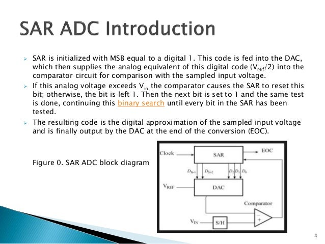
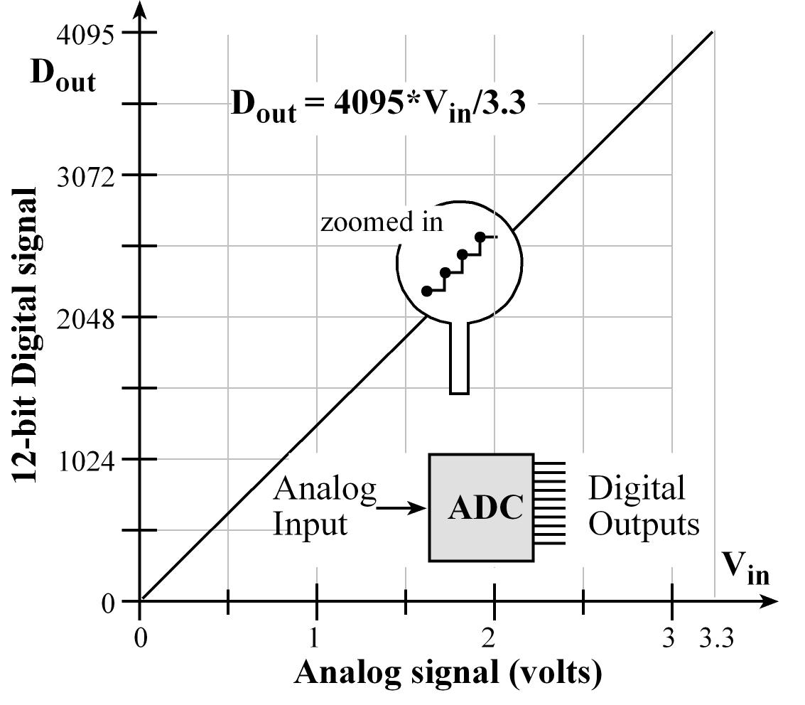
Sar adc block diagram. A Glance at the ADC IP;. A higher resolution reduces the maximum sampling rate, which is dependent on how quickly the comparator can make a decision and how fast the SAR logic can run. SAR type ADC is mostly used in digital circuit to provide interface with the microprocessor.
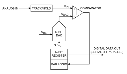
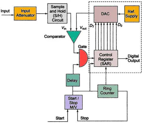
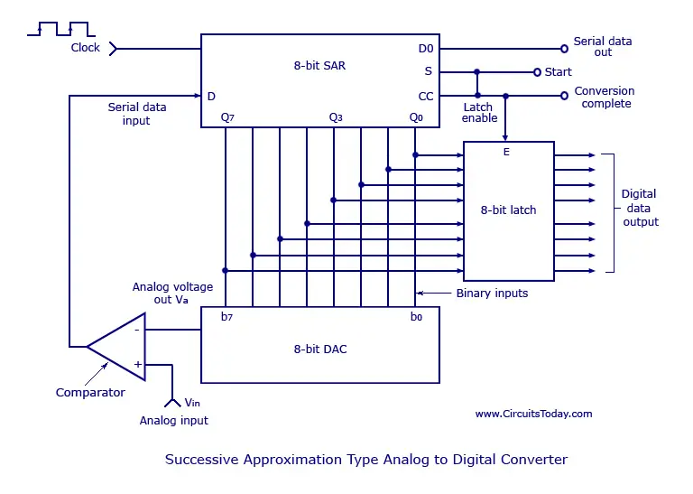
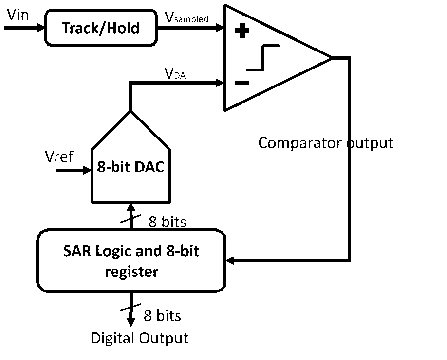
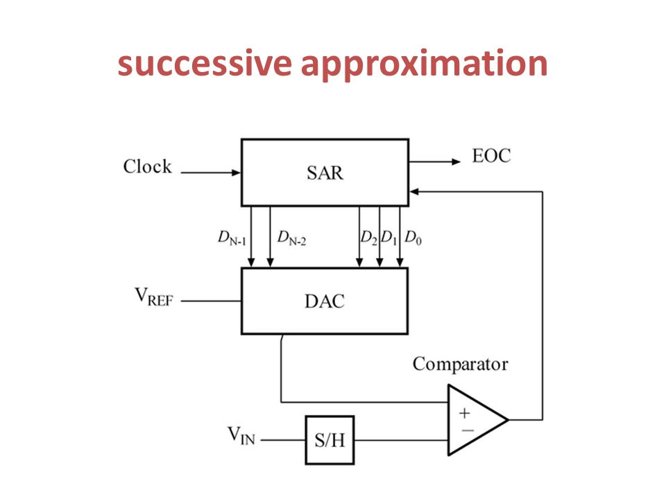
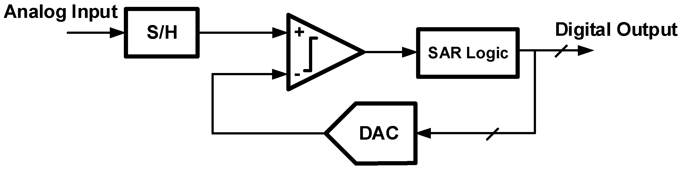
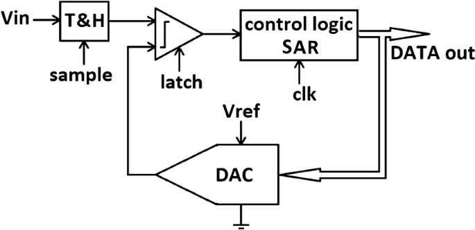
SAR ADC Block Diagram VDAC ½ 1 ¾ ¼ 0 000 001 010 011 100 101 110 111 Vin B2 = 1. In SAR type of ADC, conversion time is uniform for any analog voltage and it is equal to n*T CLK. Figure 2 The sample and hold (S/H) is used to store the input analog value for the conversion phase.
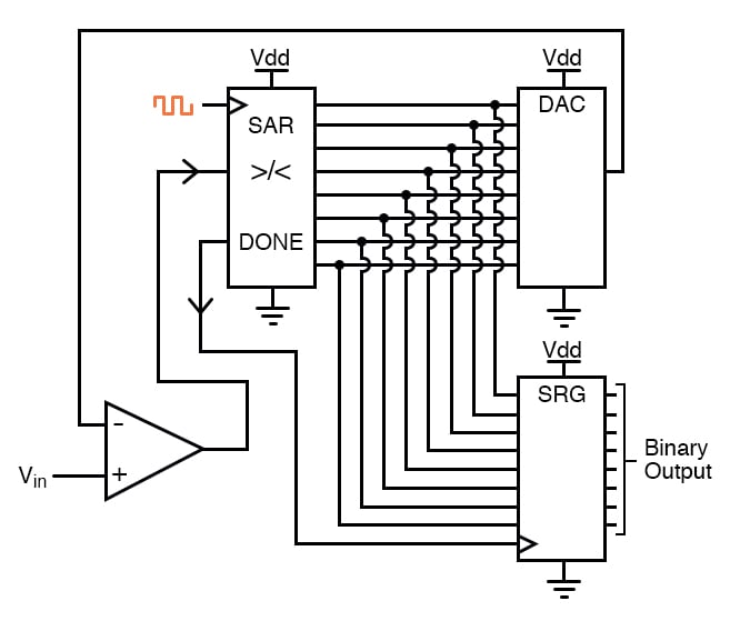
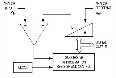
The output of SAR is given to n-bit DAC. The sample amplitude value is maintained and held in the ‘hold ‘ block. It is an analog value.
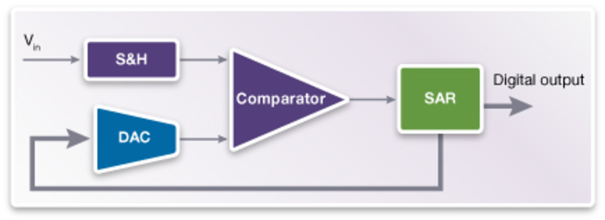
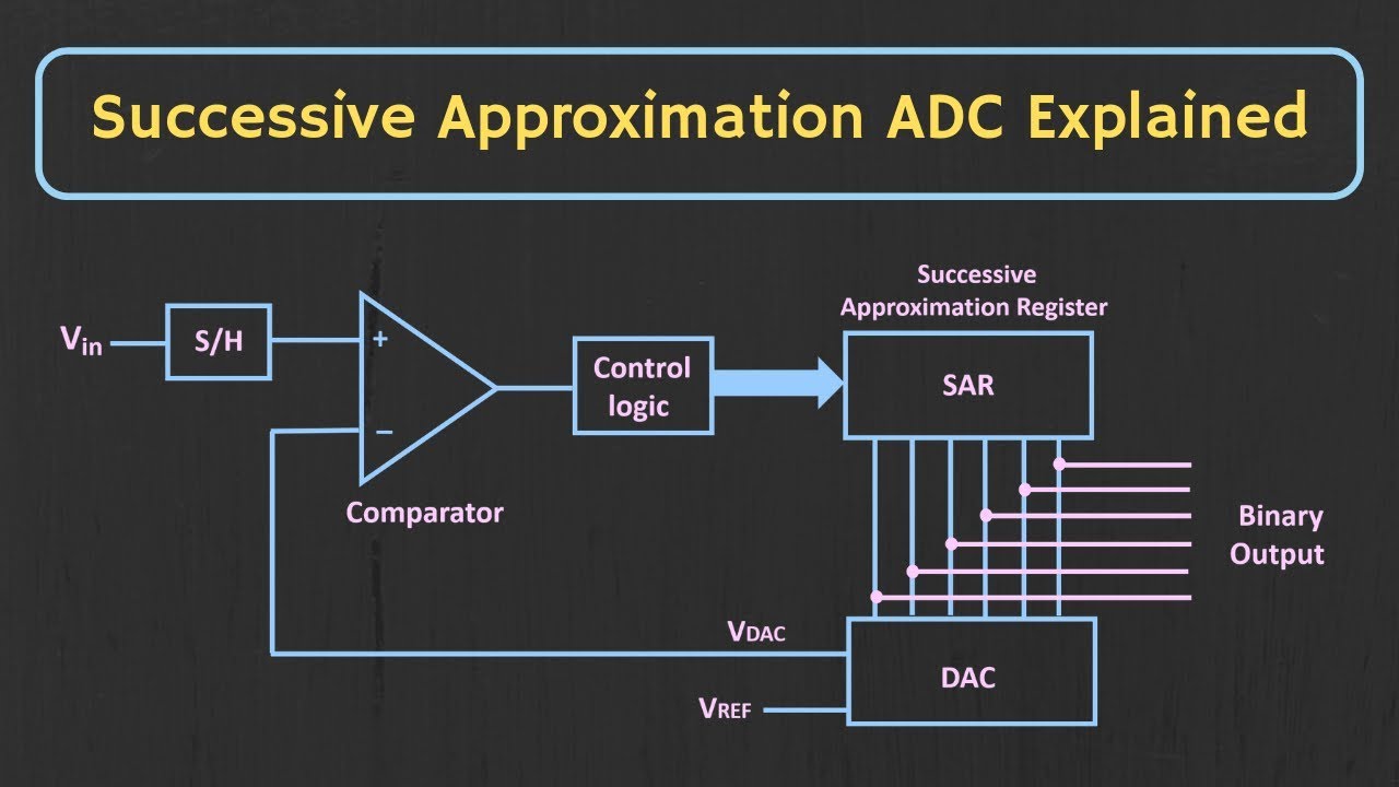
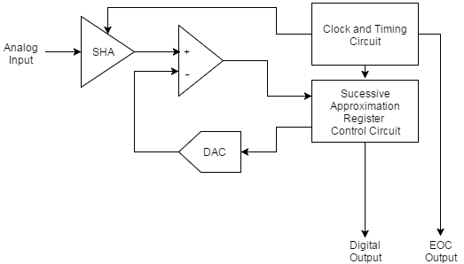
SAR ADC Block Diagram Within one sampling period, the comparator needs to make at least as many decisions as the converter resolution. SAR is the short form of Successive Approximation Register. Block Diagram of ADC The analog signal is first applied to the ‘sample‘ block where it is sampled at a specific sampling frequency.
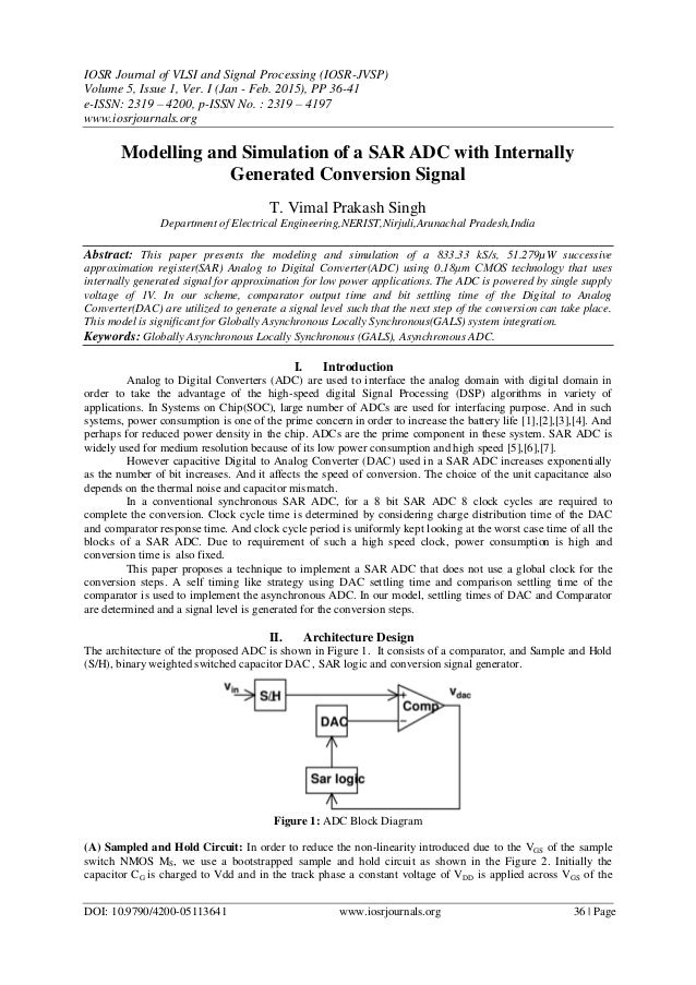
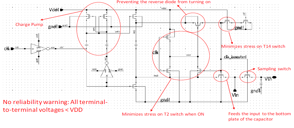
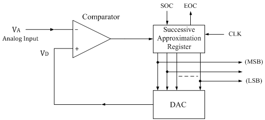
The functional block diagram of successive approximation type of ADC is shown below. The equivalent analog output voltage of DAC, VD is applied to the non-inverting input of the comparator. This repository will maintain simulation files and other relevant files of the SAR ADC block worked on in the VSD Summer Online Internship.
The analog comparator compares the S/H output with the analog threshold values generated by the digital-to-analog converter (DAC). Design yet to be modified. The simplified block diagram of a SAR ADC is shown in Figure 2.

What Is Adc Converter The Ultimate Guide Dewesoft
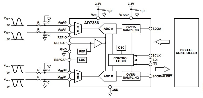
Ad7386 4 Channel 4 Msps 16 Bit Sar Adc Adi Mouser
Q Tbn 3aand9gcsecl809pbuqep2the749htbue 16ymehudodwzxdijjxkw1te6 Usqp Cau
Sar Adc Block Diagram のギャラリー

Successive Approximation Adc Ece Tutorials

12 Bit 285ks S Sar Adc W Temp Sensor
Http Www Internationaljournalssrg Org Uploads Specialissuepdf Icrtetm 19 19 Ece Ijece Icrtetm P102 Pdf
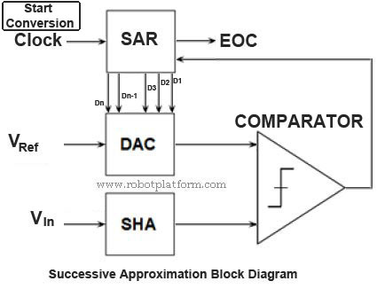
Robot Platform Knowledge Successive Approximation In Adc
.png)
Block Diagram And Working Of Adc0809 Free 8085 Microprocessor Lecture

Q Tbn 3aand9gcrl8ya0qc0rychnixqczrarrsja1gqinfvubw Usqp Cau

Design Of Hybrid Flash Sar Adc Using An Inverter Based Comparator In 28 Nm Cmos Sciencedirect

Adc Dac Tutorial Digikey

Figure 11 From An 11 Bit 250 Nw 10 Ks S Sar Adc With Doubled Input Range For Biomedical Applications Semantic Scholar

Eeblog Anh Vu
Using Sar Adc Tina Models Much Ado About Settling Precision Hub Archives Ti E2e Support Forums

Difference Between Adc Types Counter Flash Sar Dual Slope Sigma Delta
Ieeexplore Ieee Org Iel7 344 504 Pdf

Sar Adcs For Machine To Machine Connections
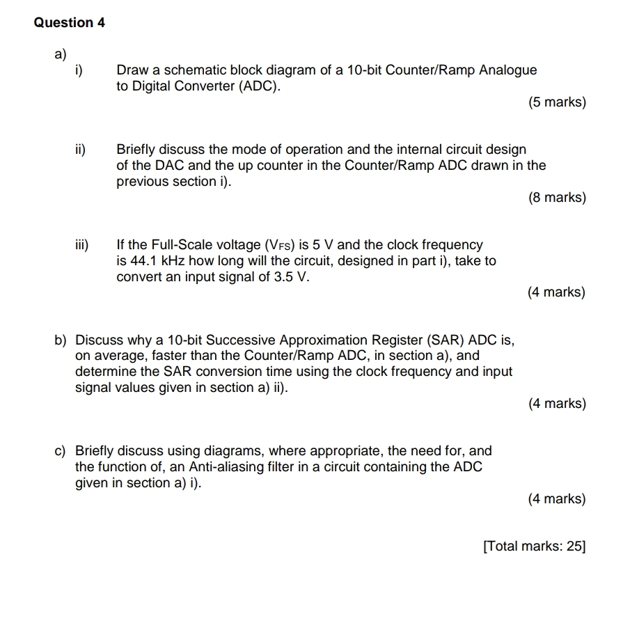
Solved Question 4 A I Draw A Schematic Block Diagram Of Chegg Com
Understanding Flash Adcs
Www Dialog Semiconductor Com Sites Default Files Precision Adcs Pdf
Diagram 8051 Adc Block Diagram Full Version Hd Quality Block Diagram Armdiagram Scacchiruta It

Guide To Understanding Successive Approximation Registers Sar And Flash Adcs Maxim Integrated

Explain 4 Bit Successive Approximation Type Adc
Guide To Understanding Successive Approximation Registers Sar And Flash Adcs Maxim Integrated
Modelling And Simulation Of A Sar Adc With Internally Generated Conve

Successive Approximation Adc The Reader Wiki Reader View Of Wikipedia
A Semi Synchronous Sar Adc With Variable Dac Settling Time Using A Dll Springerlink

Figure 1 From Design Of 9 Bit Sar Adc Using High Speed And High Resolution Open Loop Cmos Comparator In 180nm Technology With R 2r Dac Topology Semantic Scholar

What Is Adc Converter The Ultimate Guide Dewesoft
A Semi Synchronous Sar Adc With Variable Dac Settling Time Using A Dll Springerlink

Analog To Digital Convertor Adc Using Successive Approximation Technique
Developing High Performance 28 Nm Data Converters

Q Tbn 3aand9gctxxqn50jazpy8j 3doo6syeaucby87oz5bdq Usqp Cau
Analog To Digital Converter Adc Advantages Disadvantages Electricalvoice

Ad4696 Datasheet And Product Info Analog Devices
Ee6350 Vlsi Design Lab 8 Bit Sar Adc

Successive Approximation Adc Wikipedia
Successive Approximation Adc Explained Youtube
Successive Approximation Adc Digital Analog Conversion Electronics Textbook

Sar Adcs For Machine To Machine Connections

8051 Adc Block Diagram Full Hd Version Block Diagram Marv Diagram Arroccoturicchi It

Block Diagram Of Sar Adc Download Scientific Diagram
Analog To Digital Converters Successive Approximation Type Working

Learn About Sar Adcs Architecture Applications And Support Circuitry Technical Articles

Analog To Digital Converter How Adc Works With Pic Mcu

A 10 Bit 1 Ms S Segmented Dual Sampling Sar Adc With Reduced Switching Energy Sciencedirect
Jlpea Free Full Text Design Of A Programmable Passive Soc For Biomedical Applications Using Rfid Iso Nfc5 Interface Html
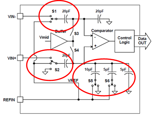
Working Of Capacitive Sar Adc
Block Diagram Of The Designed Sar Adc Download Scientific Diagram
Http Liu Diva Portal Org Smash Get Diva2 Fulltext01 Pdf
Http Raiith Iith Ac In 2570 1 Ee13m1024 Pdf

Adc Dac Tutorial Digikey
Ee6350 Vlsi Design Lab 8 Bit Sar Adc
Q Tbn 3aand9gcraqfzzx7tgyghd2mzk2mlt4kzyqyzqkruk2ajkdqq In9hpg Usqp Cau
Ads8681 16 Bit Sar Analog To Digital Converters Ti Mouser
Max 1msps Differential Sar Adc Maxim Mouser United Kingdom

Sigma Delta Adc Compared To Sar Adc Developer Help

Analog Electronics For Radiation Detection

Explain Sar Or Flash Type Adc With The Help Of A Block Diagram And Comment On Its Speed

8051 Adc Block Diagram Full Hd Version Block Diagram Marv Diagram Arroccoturicchi It

Design And Simulation Of A 6 Bit Successive Approximation Adc Using Modeled Organic Thin Film Transistors

Simplified Block Diagram Of The Successive Approximation Sar Adc Download Scientific Diagram
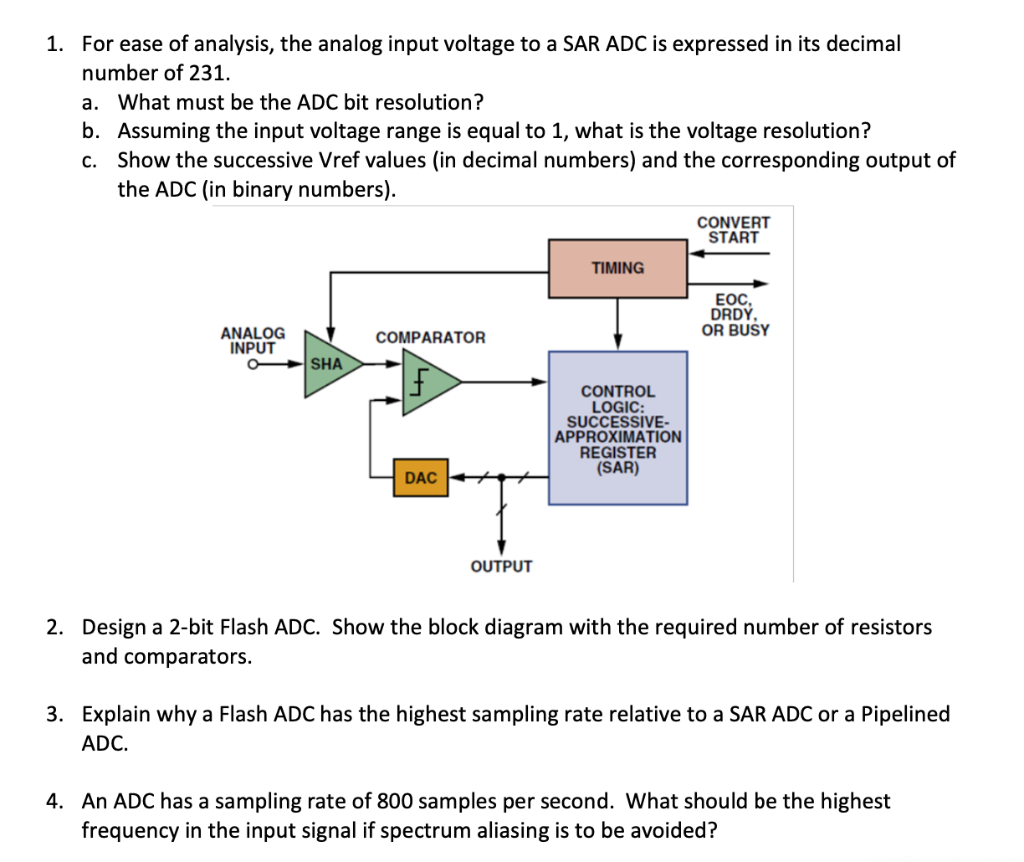
1 For Ease Of Analysis The Analog Input Voltage Chegg Com
Scholarworks Uttyler Edu Cgi Viewcontent Cgi Article 1033 Context Ee Grad
Introduction To Analog To Digital Converters Adc Predictable Designs

Functional Block Diagram Of The Proposed Sar Adc Download Scientific Diagram
Ads91 Data Sheet Product Information And Support Ti Com

Block Diagram Of A Successive Approximation Adc Download Scientific Diagram
Q Tbn 3aand9gcqh5xnyn6tdht 2wrlzrw9fk6uod Cmjiio 0k4mpq Vciwh8xv Usqp Cau
Http Atlas Physics Arizona Edu Shupe Physics Courses Phys 586 S15 S16 S17 Readings Ms Mca Readings Successive approximation adc Pdf
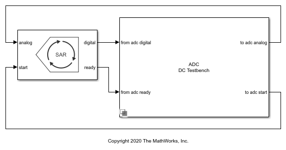
Design And Evaluate Sar Adc Matlab Simulink
Sar Adc Block Diagram 6 Download Scientific Diagram
Scholarworks Uttyler Edu Cgi Viewcontent Cgi Article 1033 Context Ee Grad
Successive Approximation Type Adc Analog Integrated Circuits Electronics Tutorial

N Bit Successive Approximation Register Sar Based Adc Simulink Mathworks Italia
Analog To Digital Converters Adc S
0808 0809 Adc Block Diagram Adc Adc0808 Adc Bit Mp Compatible A D Converters With 8 Channel Multiplexer The 8 Bit A D Converter Uses Successive Ppt Download

Air Supply Lab Analog To Digital Conveter Adc
Chapter 14 Adc Data Acquisition And Control

Design Of A New Structure Of Sar Adc Scialert Responsive Version

A 10 Bit 50 Ms S Sar Adc In 65 Nm Cmos With On Chip Reference Voltage Buffer Sciencedirect
Jlpea Free Full Text Review Of Analog To Digital Conversion Characteristics And Design Considerations For The Creation Of Power Efficient Hybrid Data Converters Html

Analog To Digital Converter How Adc Works With Pic Mcu

Understand How A Digital Multimeter Dmm Works Electronics Notes

Learn About Sar Adcs Architecture Applications And Support Circuitry Technical Articles
Adc Fasoc Fully Autonomous Soc Synthesis Using Customizable Cell Based Synthesizable Analog Circuits

Figure 1 Linearity Analysis On A Series Split Capacitor Array For High Speed Sar Adcs

Which Adc Architecture Is Right For Your Application Analog Devices

Pdf Non Binary Sar Adc With Digital Error Correction For Low Power Applications Gopi Nathan Academia Edu

Adc Dac Tutorial Digikey
Jlpea Free Full Text Review Of Analog To Digital Conversion Characteristics And Design Considerations For The Creation Of Power Efficient Hybrid Data Converters Html

The Asynchronous Sar Adc Block Diagram Download Scientific Diagram
Http Raiith Iith Ac In 2570 1 Ee13m1024 Pdf

Successive Approximation Adc Explained Youtube

Figure 1 From Blind Sar Adc Capacitor Mismatch Calibration Semantic Scholar
Direct Type Adcs Tutorialspoint
A Semi Synchronous Sar Adc With Variable Dac Settling Time Using A Dll Springerlink
10 Bit 100ks S Ulp Sar Adc

10 Bit 1ms S Sar Adc With 12 1 Input Tsmc 65nm Lp
Diagram 8051 Adc Block Diagram Full Version Hd Quality Block Diagram Armdiagram Scacchiruta It
Q Tbn 3aand9gcstc3c 63x4q Iu9x4xqempiykcm8kxp Crnkoeiof5k0mfls Usqp Cau

Block Diagram Of The 10 Bits Sar Adc Download Scientific Diagram

Pic Microcontroller Adc Module Programming In Mplab Xc8
Understanding The Successive Approximation Register Adc Technical Articles


